

Modern CPUs are very complex. There are billions of transistors inside a single processor chip, and it takes very complex techniques and advanced machinery to manufacture them.
A processor starts as a polished disc of ultra-pure silicon. It is so pure that there is roughly no more than one foreign atom for every billion silicon atoms, according to Intel itself. Hundreds of identical chip patterns are printed onto each wafer through many processes. You might have heard about the term “photolithography,” but there are many others like deposition, etching, ion implantation, and polishing. We are not going into that today.

But, after this complex manufacturing process is done, no two dies come out identical. So, all of them must be tested, graded, and sorted properly. This process of sorting is called “binning.” Manufacturers equip all of them with the same design but not all come out with everything working perfectly. If some cores are not working or the thermal performance is not up to the mark, that chip has to settle as the mid-range or low-end processor in the same generation.
So yes, sometimes a $700 Core i9 and a $250 Core i5 can come from the exact same production line starting as the same silicon wafer. It is just that they were not able to perform similarly when tested.
What is CPU binning?
This sorting process is done based on various factors like stable clock-frequency range, required voltage, and heat output.
Intel’s documentation says that there is a sequence laid out after fabrication. It says that, “When wafer processing is complete, the wafers are transferred from the fab to an assembly/test facility. There, the individual dies are first tested, then… they are singulated, and the ones that passed their test are packaged. Finally, a thorough test of the packaged part is conducted before the finished product is shipped.”
They call it the Wafer Sort Test. Processors are tested on specific parameters and sorted by them. Parameters include:
- Number of functional cores/functional units
- Maximum stable clock frequency at a given voltage
- Voltage requirement and power leakage
- Thermal characteristics
- Cache and integrated graphics functionality
Why isn’t every CPU exactly the same?
The scale at which modern processors are made is just mind-bending. Packing billions of transistors inside a chip of some centimeters can be called the best work of technology. At that scale, even a tiny dust particle, a chemical imbalance, or a misprint can ruin one transistor without touching the one right next to it. Now, if you multiply that risk by billions of transistors per chip and hundreds of chips per wafer, mistakes become almost certain.
Some chips come out flawless, while others have few or a lot of dead spots. Some just don’t work at all.

Engineers call it defect density. It tells how many flaws show up per square centimeter of silicon. The bigger the chip, the more silicon area there is for something to go wrong, and the probability increases with this. This is the reason why AMD sticks to building small chiplets rather than a giant single chip.
Leading-edge chips are increasingly printed with EUV lithography. It uses light with extremely short wavelength. The scale is so small that the patterns aren’t printed identical every time. This paper talks about the stochastic defects, which are the random print failures that show up with no obvious cause. In fact, this is one of the open challenges for the whole industry.
What happens after the chips are manufactured?
Intel largely designs and manufactures much of its silicon in its own fab, though recent genreration mix in tiles fabrication by TSMC. However, both AMD and Apple design their own chips but outsource fabrication, primarily to TSMC. But the binning process remains almost the same in all cases.
The die that hits high clocks with all cores properly working at an acceptable voltage range becomes the flagship product. The same die with non-functional cores or a lower clock ceiling becomes a lower SKU. If the core or cache numbers do not match well with the marketing numbers, some cores or caches might get disabled as well.
Processor Binning and Naming
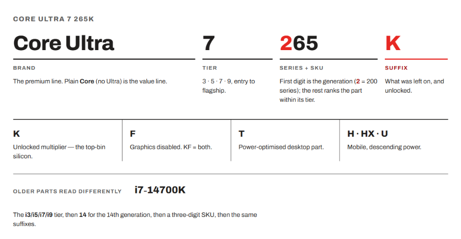
Intel’s most Core CPUs come with a fairly simple naming scheme like this: i3 (entry), i5 (mid), i7 (high-end), and i9 (flagship). They then add suffixes to them with different capabilities, like K for unlocked multiplier for overclocking, F for no integrated graphics, KF for unlocked + no iGPU, and KS for special-edition, highest-binned CPUs. Since Meteor Lake in 2023, Intel has started naming the premium chips as Core Ultra (Ultra 5/7/9 with a series 1/2/3 identifier). However, non-ultra chips are given 3/5/7 identifiers.
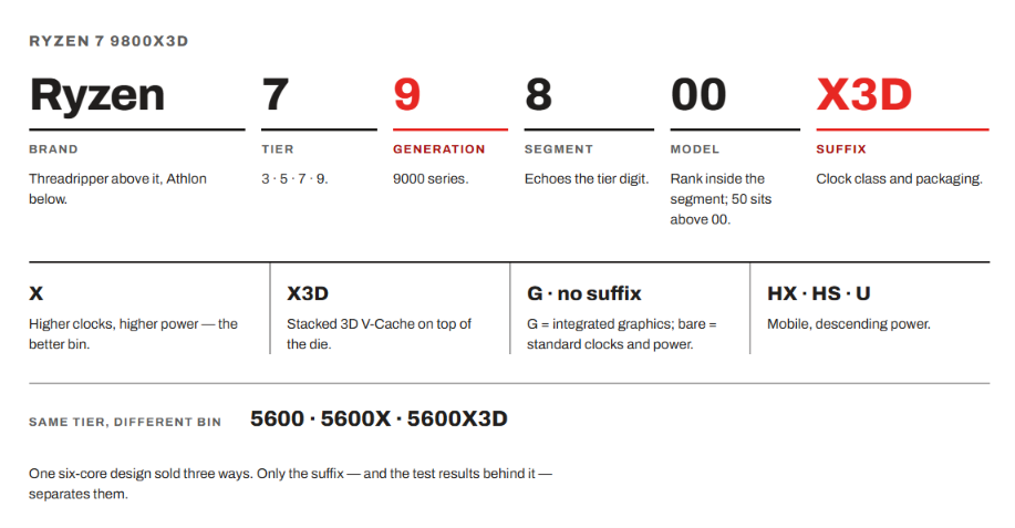
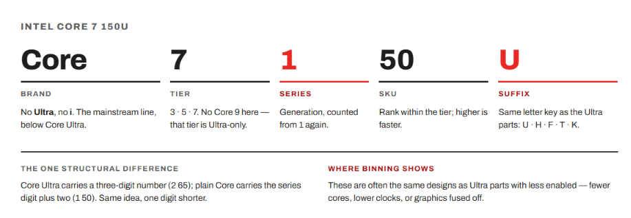
AMD has three main processor series, i.e., Ryzen 3/5/7/9 in the consumer range, Threadripper in workstations, and EPYC for servers. The latest processors have the X3D variants as well with the stacked 3D V-Cache.
The Process of Binning
We have covered the basics of manufacturing, and we don’t have to go very deep into it. So, let’s directly go to the actual binning process.
1. Testing the Silicon
Every die is tested twice after it has been out from the manufacturing unit. First, it is tested when it is still attached to the wafer. It helps catch any dead chips before cutting them out from the main wafer. After the good dies are cut away, they are tested again as a finished part.
2. Measuring Frequency, Voltage, and Power
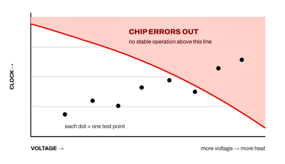
When it comes to CPU testing, it isn’t about pass or fail. There are sets of rigorous testing where engineers push speed and voltage up until the chip errors out. Where the chip fails sets the ceiling. Also, with the maximum speed, the engineers also measure how much voltage the chip needs to stay stable. Other tests are done for checking current leaks as wasted heat and how many cores and cache blocks are actually working.
There are some on-die circuits like ring oscillators and leakage-current probes that estimate the chip’s bin before it’s even packaged.
3. Sorting chips into different bins
The word “binning” comes from the grouping of similar types of processors that come out of the testing. The rules are simple. A die that hits high clock speeds at low voltage levels with all the cores working lands in the top bin. However, a die that needs more voltage, runs hotter, or has a dead core lands in a lower one.
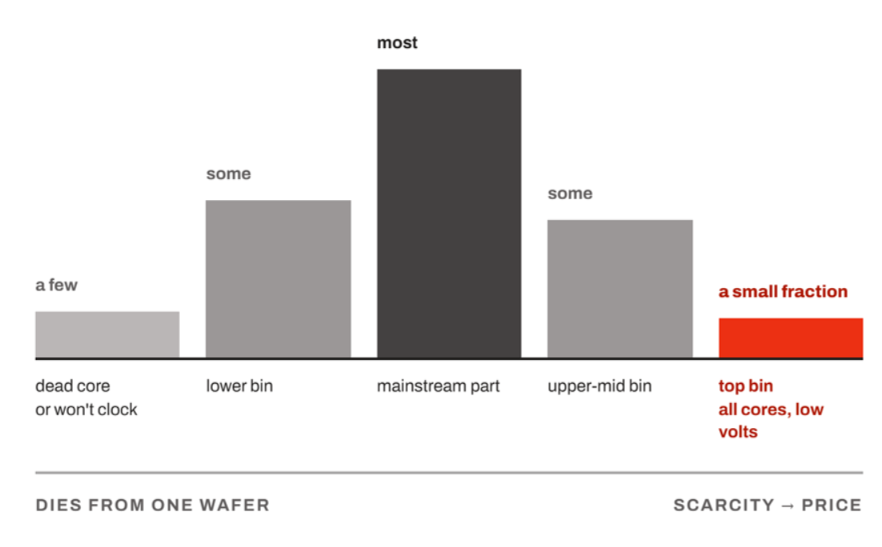
Generally, most dies land somewhere in the middle of the spectrum. A very few are found to be good enough for the top bin, and this scarcity is what makes the top-bin chips cost more.
4. Disabling defective or unneeded cores and features
Based on the bin a chip lands in, engineers decide what gets switched off. If a core is found to be defective, it will get disabled permanently. The process is generally done by eFusing (a connection that can’t be rebuilt later).
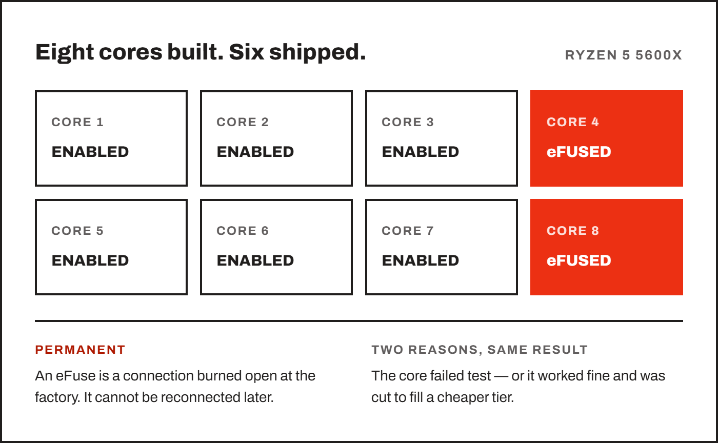
Take an example of the Ryzen 5 5600X, which comes with a chiplet that has 8 physical cores. But, two gets fused, as explained by HardwareTimes. Sometimes that core might have real defects, but there can be cases when they are disabled just to fill up a cheaper product tier.
AMD’s X3D chips are the latest example of the same idea. The Ryzen 9 7950X3D comes with two 8-core compute chiplets (CCDs), but only one of them gets the extra stacked cache. However, AMD used it smartly by routing the games to the cache-heavy chiplet while keeping other software on the faster and plain chiplet.
In the earlier times, especially in the AMD Phenom II and Athlon II era, some three-core chips were coming with four cores, with one core simply turned off. Some people were enabling that core with a motherboard feature called Advanced Clock Calibration. However, now with the eFuse technology, manufacturers have put that thing on a stop.
Conclusion
Most of the information about the CPU manufacturing, testing, and binning is kept confidential by the companies. But, we can always find really interesting things about them all the time.
So, yes, it is true that a mid-range or a budget processor in your CPU shares the same hardware as the top-end processor in its generation. It is just that it wasn’t able to deliver the highest performance and has to settle for lower performance. All thanks to CPU binning.