

I have discussed the CPU architecture in detail in this article. But this article is going to clear the confusion between the CPU architecture and microarchitecture. Most people think they both are the same, but that isn’t true. But, at the same time, they both are not independent. They are tightly connected but describe different layers of a CPU.
CPU architecture is a broader term used to describe what the CPU is designed to do and what software can expect from it. CPU microarchitecture tells how the CPU is internally designed to do it. So, if you hear someone saying that Zen 5 Ryzen has an improved IPC of approximately 16% compared to Zen 4 due to the architectural change, they are talking about the microarchitectural changes in the CPU design.
CPU architecture, usually referring to Instruction Set Architecture (ISA), defines the rules between the software and processor. It specifies things like what instructions the CPU understands, what registers are available, how instructions operate to data, or how memory is addressed, etc.
But CPU architecture isn’t just ISA. There are a lot of other things to it, and we are going to cover that in this article.
They are very low-level things attached mostly to the machine-level behavior of a CPU. x86-64, for example, is an ISA. An application of even the operating system compiled for x86-64 expects the processor to understand the instructions and basic behavior defined by the ISA.
However, CPU microarchitecture is the internal implementation of that architecture. This includes things like CPU pipeline design and depth, number and type of execution units, out-of-order execution, branch prediction, cache hierarchy, register renaming, load/store units, internal interconnects, and various other things. Now, two CPUs can use the same architecture (x86-64 or ARM64), but they can use different microarchitectures to fine-tune their products as per their philosophies. For example, Intel’s Alder Lake and AMD’s Zen 4 use different microarchitectures, but both support the x86-64 ISA.
So, we can imagine ISA as a language that defines the words and grammar that two people need to understand to communicate. The microarchitecture is how each person processes that language internally.
I don’t know who this article I am writing for is. Although understanding CPU architecture and microarchitecture is useful, the benefit depends heavily on who you are. For an average PC user, you do not need to understand details of branch prediction or reorder buffer. It can be good to know about the IPC improvements if you are about to buy a new CPU, but I have covered that in this article.
But I love explaining these topics, and I hope you will like it as well.
First, a note on terminology
People just throw “architecture” to mean different things, and this is a root of confusion for those who really want to understand this conceptually.
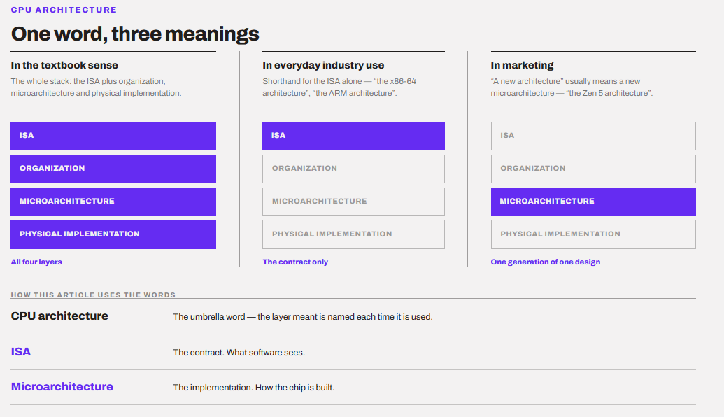
The ISA (Instruction Set Architecture) is one specific thing: the contract between software and hardware. “CPU architecture” is a broader, looser term.
In the textbook sense it means the ISA plus the organization plus the microarchitecture plus the physical implementation. In everyday industry usage, “architecture” is often just shorthand for the ISA. Most popularly, the x86-64 or ARM architecture.
And in marketing, companies say “new architecture” when they really mean “new microarchitecture” (“the Zen 5 architecture”). So, the same word can have three different meanings.
In my ISA article, I discussed a little how the word “architecture” came into the industry by IBM. They said architecture describes “the attributes of a system as seen by the programmer.” Basically, they meant the conceptual structure and functional behavior, different from the organization of the data flow and controls, the logical design, and the physical implementation.
They said, “as seen by the programmer,” which means the ISA. However, in the actual sense, the architecture of a computer is basically independent of its physical implementation. So when I use these words in this article, I mean:
- CPU architecture: The umbrella word. I will tell you which layer I mean each time.
- ISA: the contract. What software sees.
- Microarchitecture: The implementation. How the chip is built.
What is CPU architecture?
In the broader sense, CPU architecture is the overall design and organization of a CPU. It is the design both the programmer’s side and the hardware sides see. Basically, it covers what the chip promises to software and how the chip is actually built to keep that promise.
Architecture decides what capabilities it provides, how those capabilities are provided to the software, and basically how the major parts of the processor are organized to execute instructions. ISA is one layer of CPU architecture. There are more things to it, like microarchitecture and overall processor organization.
So, yes, microarchitecture is a part of CPU architecture.
Although designing the CPU architecture is a process handled by real CPU architects, engineers, product teams, and sometimes external companies, it depends on which layer we are talking about. If we talk about the ISA, such as x86-64, the ISA is controlled by the companies that own and develop that instruction-set ecosystem.
I have discussed CPU architecture (when we refer to it as an ISA) already. So, I won’t go really deep into it again. So, to be precise, all CPU manufacturers have to rely on the ISA (Instruction Set Architecture), which defines how the software communicates with the CPU. For example, x86-64, ARM64 (AArch64), and RISC-V are different CPU architectures/ISAs.
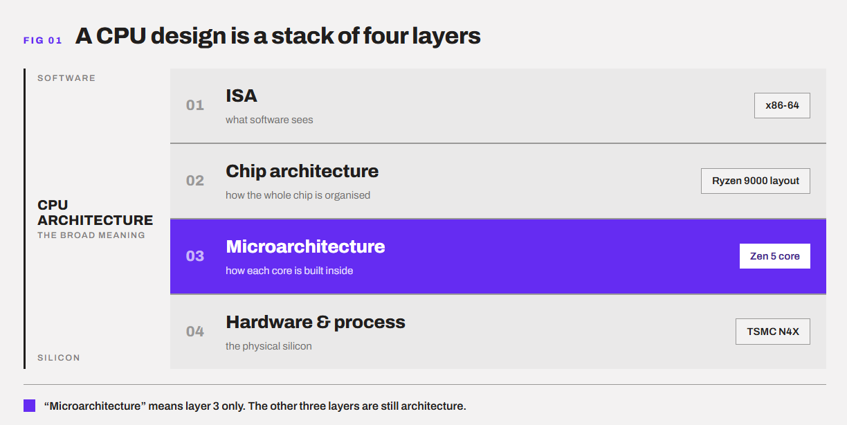
In simple terms, CPU architecture is the umbrella. Under it sit the ISA (the contract) and the microarchitecture (the implementation).
CPU architecture is a stack of layers
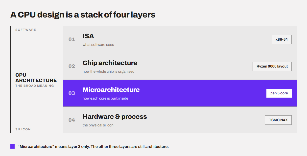
ISA is the main layer in CPU architecture, but it covers everything that software is allowed to see and depend on. Let’s get to them one by one. However, there are three more layers that we will be discussing here.
Layer 1. Instruction Set Architecture (ISA)
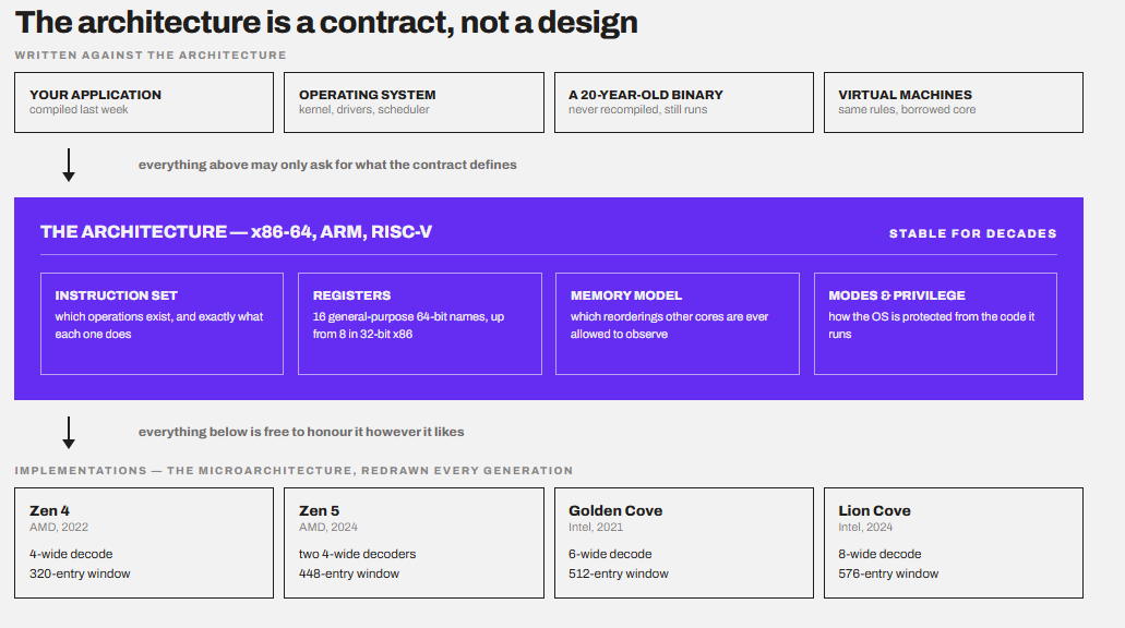
The ISA is the layer that stays fixed while everything under it changes. That is why a program that runs on a Zen 4 chip also runs on a Zen 5 chip without any change.
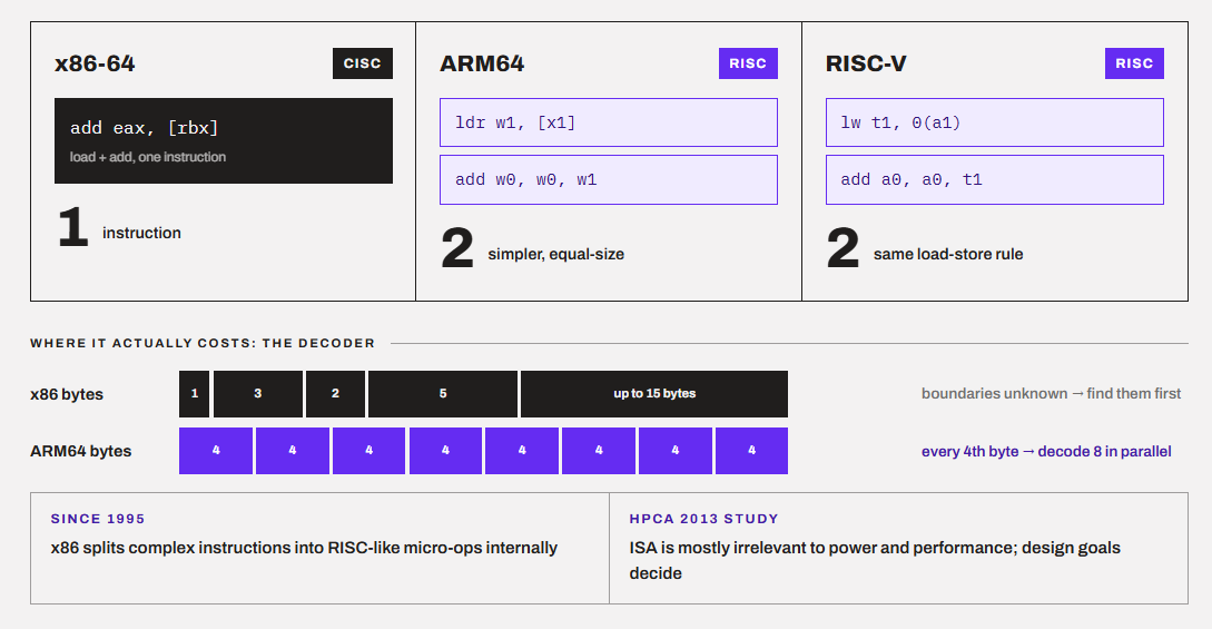
Instruction Set Architecture (ISA) is the collection of machine-level instructions that the CPU can understand and execute. The basic instructions like ADD, LOAD, SUB, STORE, etc., are ISAs. A CPU has to rely on a specific ISA to define the interface between the software and processor. x86-64, ARM64, and RISC-V are popular examples of ISA.
If that didn’t make sense, just understand that ISA is the contract between hardware and software. It defines what instructions exist, what they do, and how they are encoded in bits.
Arm’s own lead architect, Richard Grisenthwaite, put it well: the architecture is “the contract between the hardware and the software,” and it is “MUCH more than just the instruction set.”
Two different CPUs from Intel and AMD can both implement the x86-64 ISA, and they will understand the same fundamental set of instructions even though their internal design (microarchitecture) is different.
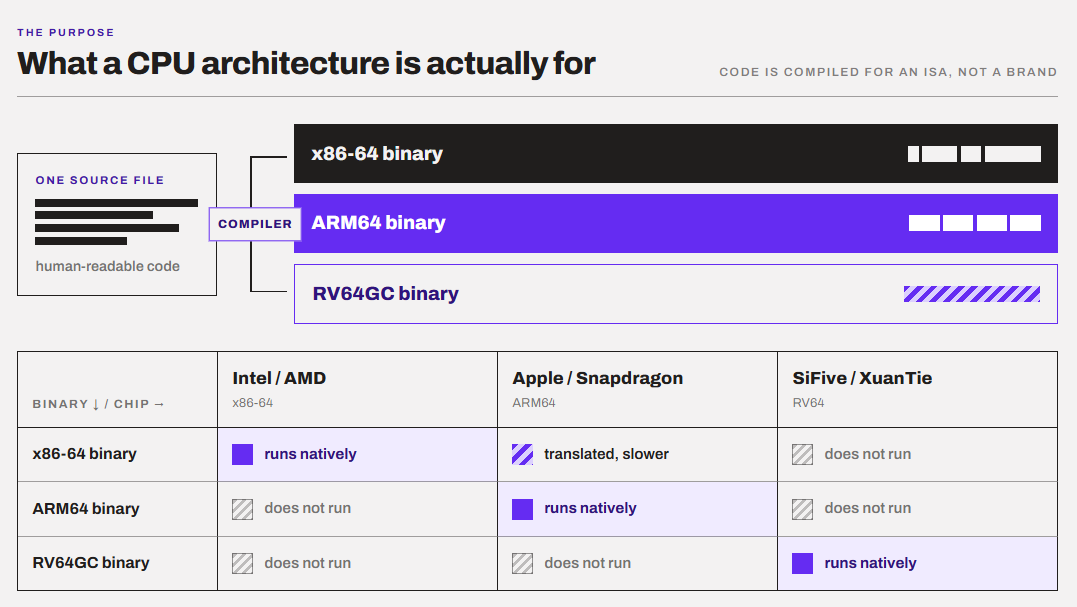
For example, most of the Intel Core and AMD Ryzen CPUs implement the x86-64 ISA. Therefore, a Windows x64 application or Windows OS itself compiled for x86-64 can generally run on both CPUs without being recompiled specifically for Intel or AMD.
However, there can be additional qualification to run the program even if the ISAs are compatible. Some software may require additional ISA extensions like AVX2 or AVX-512. A CPU must support the particular extension the program uses. To run software, the operating system can have its own requirements. Some software can be optimized for a particular CPU. For example, the Ryzen Master software won’t run on an Intel-based computer.
- ISA defines many things, and below are all of them.
- Instructions (what exists, what each does, how it’s encoded)
- Registers (how many, how wide)
- Data types Addressing modes: Memory model (ordering rules)
- Privilege levels (user vs. kernel)
- Interrupts and exceptions
- Virtual memory (page table format)
- ISA extensions (AVX2, AVX-512, SVE)
Layer 2: Chip Architecture (how the whole chip is organized)
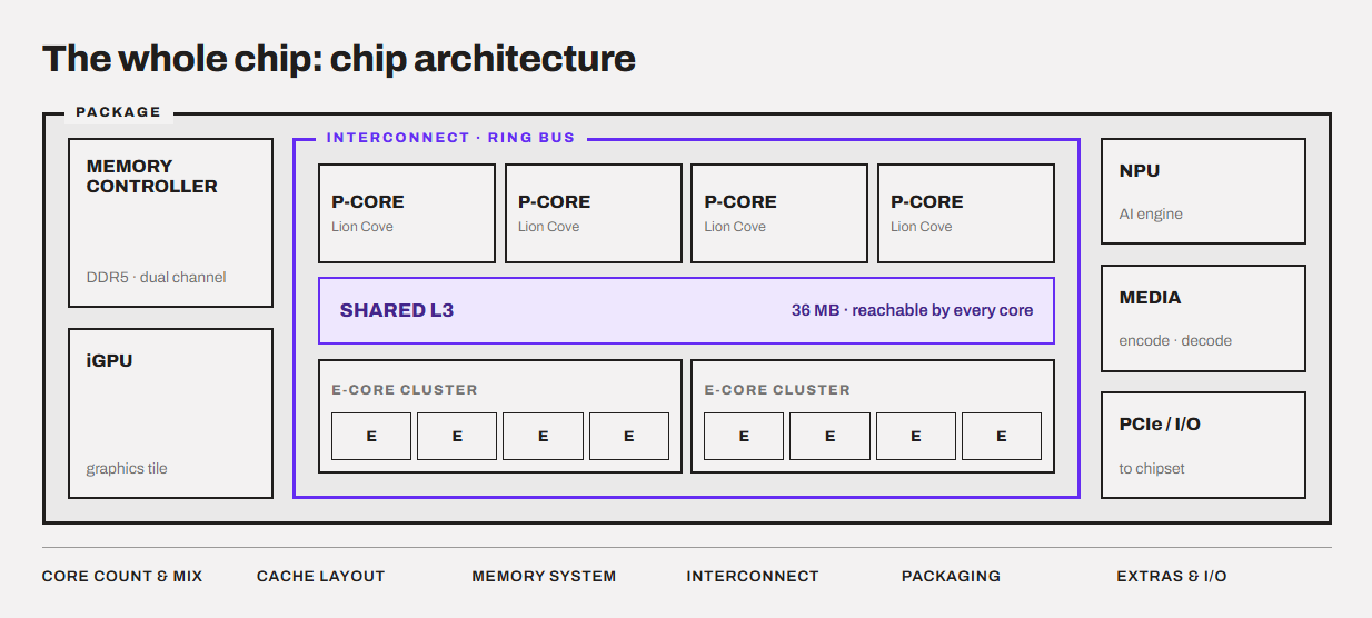
There should be a model on which the whole chip will be put together. The chip architecture decides it. It tells how many cores and which types. Also, how they share cache and how they connect, and what platform the chip sits on.
Engineers often call this the SoC or chip architecture. We will come to all the things below in this article.
Layer 3: Microarchitecture (how each core is built)
This layer decides how a core actually carries out the ISA. It decides the decoders, the branch predictors, the execution units, and the out-of-order engine. Zen 5, Lion Cove, and Skymont are names at this layer. They are core designs.
Layer 4: Hardware and process (the physical chip)
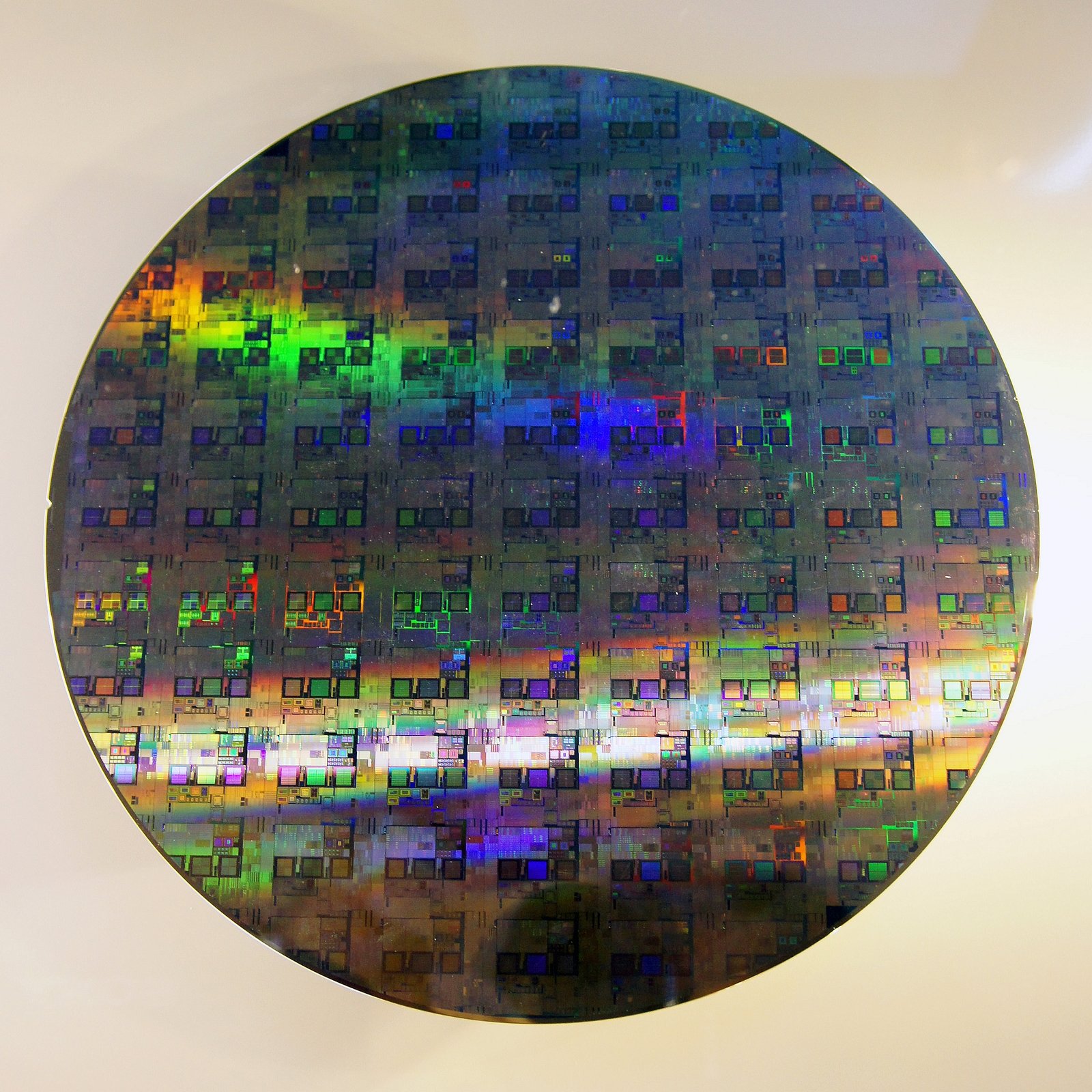
This layer is the silicon itself. This layer is about the very basic things like transistors, circuitry, and the manufacturing process that makes them. Processes like TSMC N4X and 18A come under this. It is part of the design in the textbook sense. But it is a separate choice from the other three, and we will see why that matters later.
What depends on chip architecture?
The Layer 2 demands some more room in our article because these are decisions made for the whole chip and not for a single core.
1. Core count and core mix (how many, which kinds)
The chip design decides how many cores there are and whether they are all the same type or different. For example, Intel’s Core Ultra 9 285K has 8 performance cores (Lion Cove) and 16 efficiency cores (Skymont). This is all a result of a distinct chip-level design. However, how each of those cores works inside is the microarchitecture.
2. Cache Layout
For cache, the chip architecture mainly decides its layout. It tells which cache is private to each core and which is shared and between whom. For example, in in Zen 5, each 8-core chiplet shares one 32 MB L3 cache. On Arrow Lake, each P-core gets its own L2, the E-cores share L2 in clusters of four, and all of them share one L3.
The architecture decides who shares what. But the microarchitecture decides how big, how fast, and how it is built.
3. Memory System
This part mainly decides how the CPU reaches your RAM. Things like the memory type and memory channels are decided by the chip architecture. Current AM5 and LGA1851 desktop chips are dual-channel DDR5. However, there can be other designs such as Apple M-series chips where the CPU and GPU share one pool of RAM.
4. Interconnect
Interconnect is the road by which cores, caches, and memory talk to each other. Different CPUs use different types of interconnects. Intel desktop chips use a ring bus, a loop that links the cores and the L3. Big Xeon server chips use a mesh, a grid that scales better with many cores. AMD links its chiplets with Infinity Fabric.
The interconnect affects how quickly one core can reach data another core is using. That is why core-to-core latency sometimes shows up in reviews. More on how cores work together in single-core vs. multi-core performance.
5. Monolithic vs. Chiplet
The chip design also decides whether the processor will be in one piece or multiple pieces in a single package. If the chip is monolithic, it puts everything on one die. On the other hand, the chiplet design split it. For example, the Ryzen 9000 uses one or two core chiplets (CCDs) plus a separate I/O die. Arrow Lake uses the tiles strategy with a compute tile, a GPU tile, an SoC tile, and an I/O tile, placed on a base using Intel’s Foveros packaging.
The reason for splitting a chip into pieces affects the cost of the chip, yield, and latency. However, unlike the popular opinion, it has nothing to do with how a single core decodes instruction.
6. Integrated components (iGPU, NPU, etc.)
The chip architecture decides what else lives on the chip besides the CPU cores. Most chips now have integrated graphics able to do pretty good jobs of a graphics engine. Many add an NPU, a small engine for AI tasks. Arrow Lake desktop chips have one in the SoC tile. Video encode and decode engines sit here too.
Again, unlike most people think, none of these are part of the core microarchitecture. They are separated blocks placed on the chip.
7. I/O and platform
This part decides how the chip connects to the rest of your PC. Things like chipset, PCIe lanes and their generation, USB, and the socket. Ryzen 9000 uses AM5. Core Ultra 200S uses LGA1851. The socket decides which motherboards work and often how long the platform lasts.
For an end user, this is one of the key decisions when looking to upgrade or buy a new CPU. A great core means little if the platform is dead after one generation. I have talked about platform longevity in my AMD vs Intel article.
8. Design Family
Every chip belongs to a family. Zen is a family. Intel’s “Cove” P-cores are a family. The family carries ideas forward, while the core inside gets reworked each generation. That is why Zen 4 and Zen 5 feel related but perform differently.
What is CPU microarchitecture?
When we talk about CPU microarchitecture, we basically zoom into a CPU core.
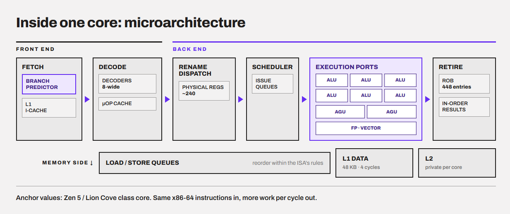
Microarchitecture is how a core is built to carry out the ISA. The ISA says what instructions exist. The microarchitecture decides how quickly and efficiently the core gets through them. Let’s discuss each part of it. I will keep them short.
1. Front-end decoders
The front end fetches instructions and decodes them into smaller internal operations called micro-ops. Width is the most important thing here. For example, Zen 4 decodes 4 instructions per cycle, while Zen 5 uses two 4-wide decode units. Intel’s Golden Cove decodes 6 per cycle, and Lion Cove decodes 8.
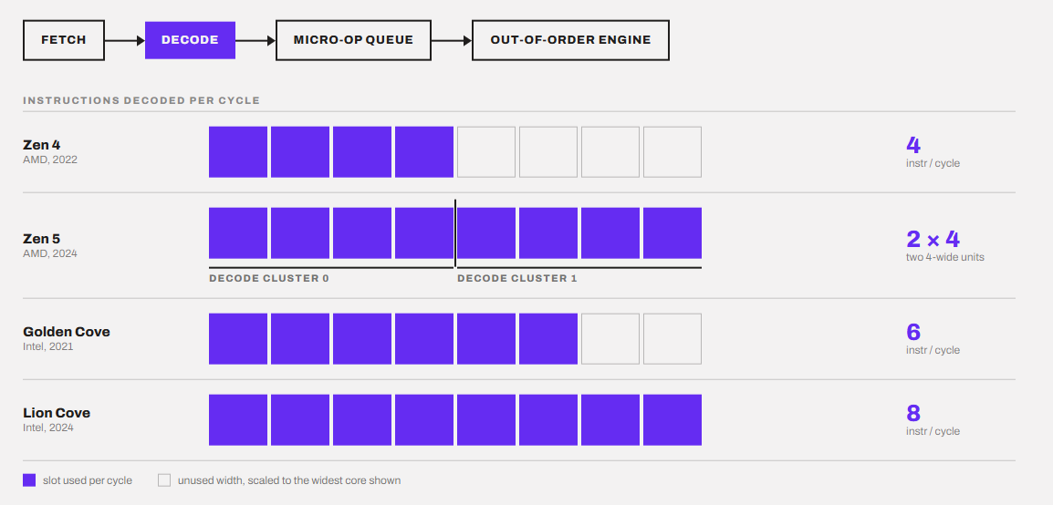
This basically tells you how much instruction-processing capability the CPU has before the instruction reaches the out-of-order execution engine. A wider front end can surely feed more work into the back end but only help with performance if the front end is not actually a bottleneck. So, do not think a wider front-end decoder always means better performance.
2. Branch predictor
A CPU guesses which way a branch (an if/else or a loop) will go before it knows for sure, so the pipeline doesn’t stay idle for long. This results in waste of CPU resources.
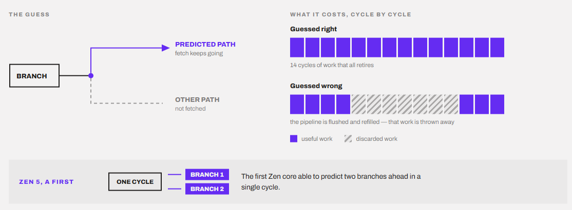
Better guesses mean fewer wasted cycles. Zen 5 was the first Zen core able to predict two branches ahead in one cycle. If you want to see why this matters so much, read A Deep Dive into CPU Pipelining.
3. Execution Units
This is where the actual work happens. The execution unit is a combination of integer ALUs, address units, floating-point pipes, etc.
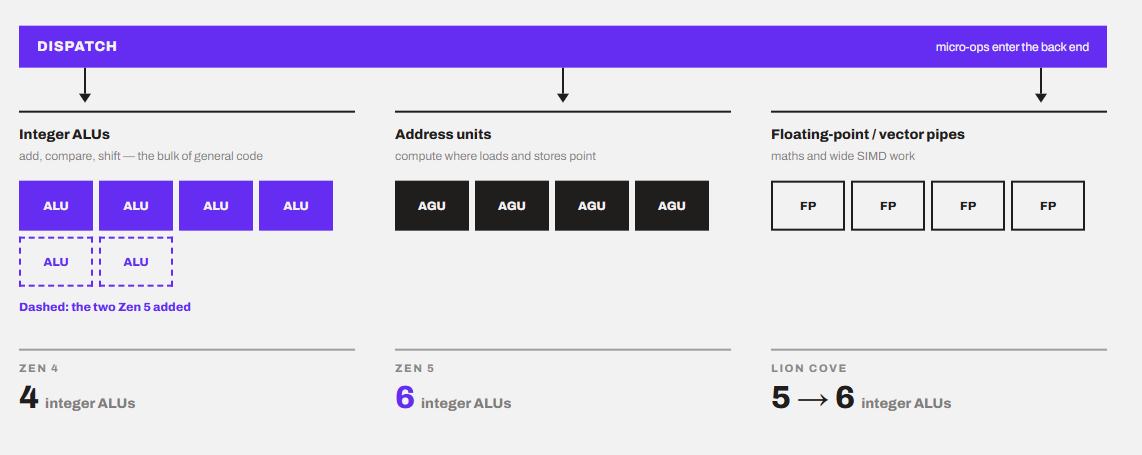
More execution units means more work done per cycle. Zen 4 has 4 integer ALUs. Zen 5 has 6. Lion Cove also moved from 5 to 6 ALUs.
4. Physical Registers and Register Renaming
The x86-64 architecture provides software with 16 general-purpose 64-bit registers. It has doubled the 8 general-purpose registers available in the older 32-bit x86 architecture. But, inside the core, there are far more of them. Read more about the difference between x86 and x86-64.
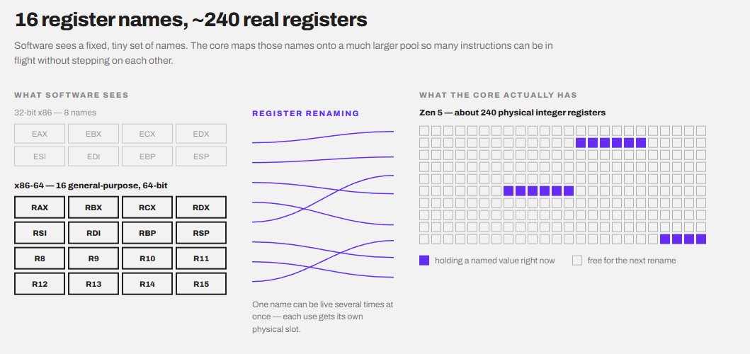
For example, a Zen 5 core has around 240 physical registers for integers alone. The core quietly maps the 16 register names onto them. This trick is called register renaming. It simply lets many instructions work at the same time without stepping on each other.
5. Out-of-order engine
The real order is never concise. It has gaps. One instruction may have to wait for the data while the other one is actively being run. A CPU can keep working on other instructions while one instruction is waiting.
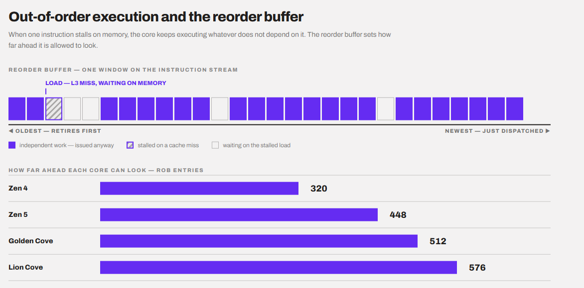
The reorder buffer (ROB) sets how far ahead the core can look. Zen 4 has 320 entries. Zen 5 has 448. Golden Cove has 512, and Lion Cove has 576.
So, basically, a larger ROB can help the CPU find more independent work when earlier instructions are stalled. This can help with performance on workloads with long-latency operations such as cache misses.
6. Cache Design (Size, Speeed, and Structure)
We discussed above that the chip architecture decides who shares which cache. But core design decides how each cache is built, its size, associativity, and latency.
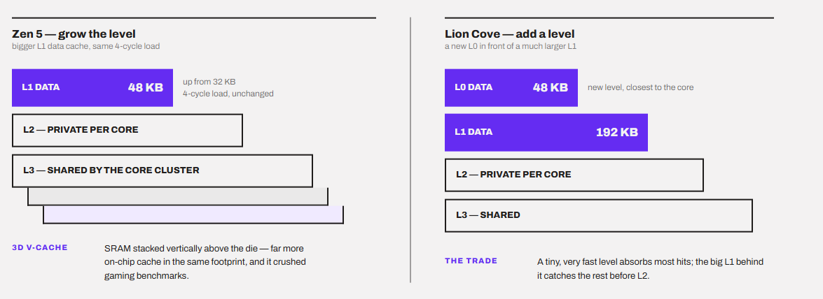
Zen 5 grew its L1 data cache from 32 KB to 48 KB while keeping a 4-cycle load. Lion Cove went further and added a new level. It now has a 48 KB L0 data cache and a 192 KB L1 data cache before the L2. AMD’s 3D V-Cache is an impressive example of a good cache design. AMD took this further by increasing the amount of on-chip cache through vertically stacked SRAM, which just crushed all gaming benchmarks.
7. Load-store queues, micro-op cache, dispatch, and retire
The load-store queues hold memory reads and writes while they are in flight. The core reorders them for speed, but always within the rules of the ISA’s memory model. So, an x86 core can reorder a lot internally. It just has to make sure other cores never see the result in a way x86 forbids.
Decoded micro-ops are kept in a micro-op cache so the core does not have to decode them again. Dispatch is how many ops enter the back end per cycle. Retire is how many finish per cycle.
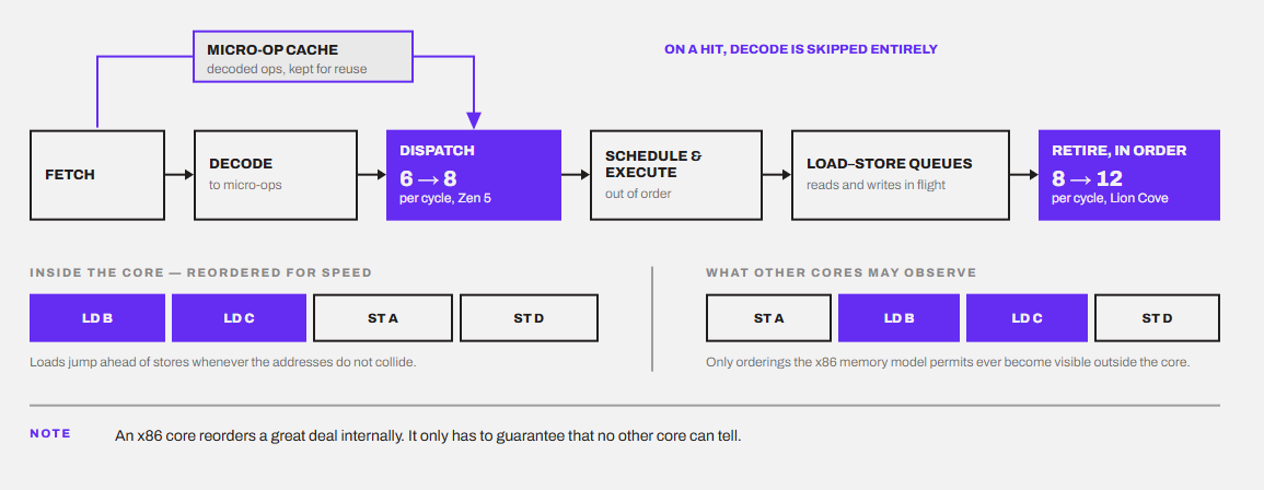
Zen 5 widened dispatch from 6 to 8 per cycle. Lion Cove retires up to 12 per cycle, up from 8.
8. SMT support
Whether one core can run two threads at once is also a core design decision.
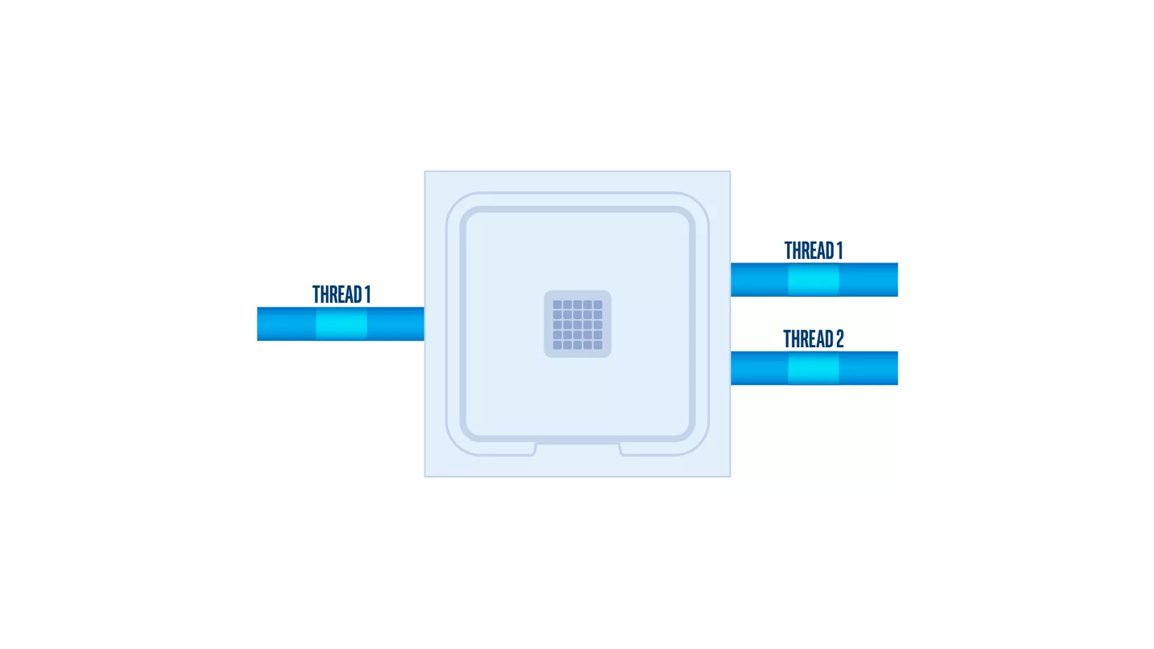
Zen 5 keeps SMT. Lion Cove removed Hyper-Threading completely. More on this in How do CPU threads work? SMT vs. Hyperthreading.
Where does the line get blurry?
If I be honest, the line between chip architecture and microarchitecture is not perfectly sharp.
Hennessy and Patterson place the memory system and the interconnect under “organization,” which they treat as microarchitecture. So a textbook would put some of the chip-level list above under microarchitecture too.
The industry is somewhat clear in this. They mostly draw the line at the core. Microarchitecture is how one core is built. Chip architecture is how the whole chip is organized around those cores. That is the split I use in this article, and it matches how AMD and Intel name things.
I think you will understand it better with this example.
A Ryzen 5 9600X and a Ryzen 9 9950X both use Zen 5 cores. They have the same microarchitecture. But the 9600X has 6 cores on one chiplet, and the 9950X has 16 cores across two. The difference is at the chip level, not inside the core.
Why does microarchitecture matter to you as a buyer?
To be precise, microarchitecture is why a new CPU is faster at the same clock speed. It is the real reason why we see a higher IPC in the newer CPU generations.
Clock speed tells you how many cycles happen per second. But there is a limit to scaling the core clock. IPC tells you how much work gets done per cycle. The microarchitecture sets the IPC. And, we can improve IPC significantly with improvements in the microarchitecture.
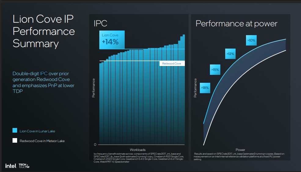
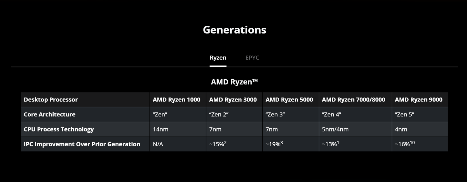
Imagine two cores locked at 4.0 GHz. One is Zen 4, and one is Zen 5. Same clock, same ISA, same software. The Zen 5 core still gets through about 16% more work on average because it decodes more, predicts better, and keeps more instructions in flight.
That gap is pure microarchitecture.
So, when you shop, the generation of the core usually tells you more about real speed than the GHz number. But the chip architecture still matters. Core count, cache layout, and platform decide whether that fast core comes with the right features for you.
Common confusions and clarifications
“Zen 5 architecture” vs. “Zen 5 microarchitecture”
Neither is really wrong here. But Zen 5 is a core design, so “microarchitecture” is the precise word here. “Architecture” is just loose marketing work thrown around. When you read about it, treat Zen 5, Lion Cove, and Skymont as core microarchitectures.
Codename vs. microarchitecture
Most people think “Granite Ridge” or “Arrow Lake” is the microarchitecture. But it isn’t. Those are chip codenames.
Granite Ridge is the Ryzen 9000 desktop chip, and the core inside is Zen 5. Arrow Lake is the Core Ultra 200S chip, and the cores inside are Lion Cove and Skymont. So one chip codename can hold two microarchitectures. In fact, some Arrow Lake laptop chips even hold three: Lion Cove, Skymont, and Crestmont low-power cores.
Process node vs. microarchitecture
I have seen people reading “4nm” or “3nm” as if it describes the design. It isn’t. The node is the manufacturing process, layer 4 in our stack. In fact, the same core can be designed on different nodes.
For example, AMD builds regular Zen 5 on TSMC N4X and the compact Zen 5c version on a 3 nm-class node. Another example is when Intel took its 10 nm Sunny Cove core and rebuilt it on 14 nm as Cypress Cove for 11th Gen desktop chips.
Conclusion
If you want to stay away from confusions, just remember the stack. The ISA on top, then the chip architecture, then the microarchitecture, then the hardware and process underneath.
“CPU architecture” in the full sense is the whole stack. Microarchitecture is only the core layer, but it is where most of the performance gains of the last decade came from.
There can be things that belong to both, such as registers and the memory model; just use one test. If software can see it, it is ISA. If it is hidden machinery that makes the ISA fast, it is microarchitecture.
I hope this helps.